- 您现在的位置:买卖IC网 > Sheet目录337 > LE25U20AMB-AH (ON Semiconductor)IC MEM 2MBIT SERIAL FLASH 8SOP
�� �
�
�LE25U20AMB�
�WEN� (bit� 1)�
�The� WEN� register� is� for� detecting� whether� the� device� can� perform� write� operations.� If� it� is� set� to� "0",� the� device� will� not�
�perform� the� write� operation� even� if� the� write� command� is� input.� If� it� is� set� to� "1",� the� device� can� perform� write�
�operations� in� any� area� that� is� not� block-protected.�
�WEN� can� be� controlled� using� the� write� enable� and� write� disable� commands.� By� inputting� the� write� enable� command�
�(06h),� WEN� can� be� set� to� "1";� by� inputting� the� write� disable� command� (04h),� it� can� be� set� to� "0".� In� the� following� states,�
�WEN� is� automatically� set� to� "0"� in� order� to� protect� against� unintentional� writing.�
�?� At� power-on�
�?� Upon� completion� of� small� sector� erase,� sector� erase� or� chip� erase�
�?� Upon� completion� of� page� program�
�?� Upon� completion� of� status� register� write�
�*� If� a� write� operation� has� not� been� performed� inside� the� LE25U20AMB� because,� for� instance,� the� command� input� for�
�any� of� the� write� operations� (small� sector� erase,� sector� erase,� chip� erase,� page� program,� or� status� register� write)� has�
�failed� or� a� write� operation� has� been� performed� for� a� protected� address,� WEN� will� retain� the� status� established� prior� to�
�the� issue� of� the� command� concerned.� Furthermore,� its� state� will� not� be� changed� by� a� read� operation.�
�BP0,� BP1� (bits� 2,� 3)�
�Block� protect� BP0� and� BP1� are� status� register� bits� that� can� be� rewritten,� and� the� memory� space� to� be� protected� can� be�
�set� depending� on� these� bits.� For� the� setting� conditions,� refer� to� "Table� 4� Protect� level� setting� conditions".�
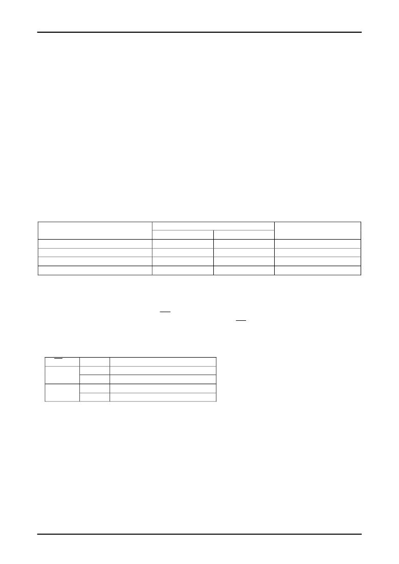
�Table� 4� Protect� Level� Setting� Conditions�
�Protect� Level�
�BP1�
�Status� Register� Bits�
�BP0�
�Protected� Area�
�0� (Whole� area� unprotected)�
�1� (1/4� protected)�
�2� (1/2� protected)�
�3� (Whole� area� protected)�
�0�
�0�
�1�
�1�
�0�
�1�
�0�
�1�
�None�
�30000h� to� 3FFFFh�
�20000h� to� 3FFFFh�
�00000h� to� 3FFFFh�
�*� Chip� erase� is� enabled� only� when� the� protect� level� is� 0.�
�SRWP� (bit� 7)�
�Status� register� write� protect� SRWP� is� the� bit� for� protecting� the� status� registers,� and� its� information� can� be� rewritten.�
�When� SRWP� is� "1"� and� the� logic� level� of� the� WP� pin� is� low,� the� status� register� write� command� is� ignored,� and� status�
�registers� BP0,� BP1,� and� SRWP� are� protected.� When� the� logic� level� of� the� WP� pin� is� high,� the� status� registers� are� not�
�protected� regardless� of� the� SRWP� state.� The� SRWP� setting� conditions� are� shown� in� "Table� 5� SRWP� setting� conditions".�
�Table� 5� SRWP� Setting� Conditions�
�WP� Pin�
�0�
�1�
�SRWP�
�0�
�1�
�0�
�1�
�Status� Register� Protect� State�
�Unprotected�
�Protected�
�Unprotected�
�Unprotected�
�Bits� 4,� Bits� 5,� and� Bits� 6� are� reserved� bits,� and� have� no� significance.�
�No.A2097-9/21�
�发布紧急采购,3分钟左右您将得到回复。
相关PDF资料
LFDAS12XSIT
HARDWARE MC9S12XS 112-PIN
LFXP10E-L-EV
BOARD EVAL LATTICEXP10E STD
LH28F008SCHT-TE
IC FLASH 8MBIT 85NS 40TSOP
LH28F160S3HNS-TV
IC FLASH 16MBIT 100NS 56SSOP
LH28F160S5HNS-S1
IC FLASH 16MBIT 70NS 56SSOP
LH28F320S3HNS-ZM
IC FLASH 32MBIT 110NS 56SSOP
LH28F320SKTD-ZR
IC FLASH 32MBIT 70NS 48TSOP
LHF00L28
IC FLASH 16MBIT 70NS 48TSOP
相关代理商/技术参数
LE25U20AMBM02-AH
功能描述:闪存 RoHS:否 制造商:ON Semiconductor 数据总线宽度:1 bit 存储类型:Flash 存储容量:2 MB 结构:256 K x 8 定时类型: 接口类型:SPI 访问时间: 电源电压-最大:3.6 V 电源电压-最小:2.3 V 最大工作电流:15 mA 工作温度:- 40 C to + 85 C 安装风格:SMD/SMT 封装 / 箱体: 封装:Reel
LE25U40CFQ-AH
制造商:ON Semiconductor 功能描述:REEL / S-FLASH MEMORY(4M)
LE25U40CMC
制造商:SANYO 制造商全称:Sanyo Semicon Device 功能描述:4M-bit (512K??8) Serial Flash Memory
LE25U40CMC-AH
功能描述:闪存 S-FLASH MEMORY(4M)
RoHS:否 制造商:ON Semiconductor 数据总线宽度:1 bit 存储类型:Flash 存储容量:2 MB 结构:256 K x 8 定时类型: 接口类型:SPI 访问时间: 电源电压-最大:3.6 V 电源电压-最小:2.3 V 最大工作电流:15 mA 工作温度:- 40 C to + 85 C 安装风格:SMD/SMT 封装 / 箱体: 封装:Reel
LE25U40CMCQ00-AH
制造商:ON Semiconductor 功能描述:Flash S-FLASH MEMORY(4M)
LE25U40CQE
制造商:SANYO 制造商全称:Sanyo Semicon Device 功能描述:4M-bit (512K??′8) Serial Flash Memory
LE25U40CQE-AH
功能描述:电可擦除可编程只读存储器 RoHS:否 制造商:Atmel 存储容量:2 Kbit 组织:256 B x 8 数据保留:100 yr 最大时钟频率:1000 KHz 最大工作电流:6 uA 工作电源电压:1.7 V to 5.5 V 最大工作温度:+ 85 C 安装风格:SMD/SMT 封装 / 箱体:SOIC-8
LE25U40CQES00-AH
制造商:ON Semiconductor 功能描述:S-FLASH MEMORY(4M)